With the rapid commercialization of the Internet of Things, cloud computing, 5G communication, and intelligent driving, the market demand for high-performance computing chips has shown explosive growth, which has directly promoted the significant increase in chip power consumption. FCBGA packaging technology has become the mainstream solution for high-end chip packaging.
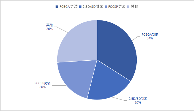
According to the data of Guanyan Tianxia, from the perspective of global market size, the global advanced packaging market will reach 51.900 billion US dollars in 2024, a year-on-year increase of 10.9%; The global advanced packaging market is expected to reach $57.1 billion by 2025. From the perspective of market structure, the advanced packaging market is dominated by FCBGA, accounting for 34%; 2.5D/3D packaging and FCCSP packaging both account for 20% of the global market.

Figure 1 Global advanced packaging market size (compiled by HFC based on public information)
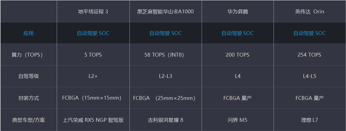
At present, the competitive landscape of the global and Chinese ADAS (advanced driver assistance system) chip market presents the dual characteristics of "foreign giants dominate the rise of local manufacturers", NVIDIA, Qualcomm and Mobileye have been recognized by the market in the world, and the domestic market is dominated by Huawei, Horizon and Black Sesame Intelligence.

Figure 2 ASDS intelligent driving chip designed with FCBGA package (compiled by HFC based on public information)
● High-density interconnect: The flip chip design shortens the electrical interconnection distance, supports more I/O pins, reduces parasitic effects, and improves high-frequency signal integrity and accuracy.
● Efficient heat dissipation: More than 90% of the heat is directly conducted from the lid to the external radiator during the calculation process. The effective heat dissipation area and low thermal resistance of the TIM and Lid of the heat dissipation path are critical.
● High integration: 10-layer cabling supports complex power supply/signal networks, and the low-profile design meets the space constraints of vehicle/mobile devices.
● Long-term reliability: Underfill material improves mechanical strength, TIM material provides long-term stable heat transfer, and Lid cover provides dual protection of heat dissipation and mechanical compression and vibration resistance.

Fig.3. Schematic cross-section of a typical FCBGA with a Lid lid structure
FCBGA package
Challenges in heat dissipation technology and material innovation
As the mainstream packaging solution for high-performance chips, the computing power and power consumption of chips are rising, which puts forward higher requirements for the heat dissipation efficiency and long-term computing reliability of FCBGAs. With the popularization of AI acceleration chips and high-end intelligent driving SOC chips, the heat flux density and chip size of mainstream chips have increased significantly, and the traditional heat dissipation material system is facing fundamental challenges.
Traditional materials (silicone grease, indium flakes) face many difficulties in large-size and high-power FCBGA packaging applications:
● Silicone grease
Low thermal conductivity: The thermal conductivity is only 3-6W/m·K, which is difficult to cope with high heat flux scenarios.
Material risk: Long-term use has the problem of drying out and aging, resulting in a non-linear increase in interfacial thermal resistance (TIM resistance). Low coverage of large packages.
● Indium sheets
Process bottleneck: Although it has high thermal conductivity of 86 W/m·K, it requires complex processes such as flux spray and vacuum reflow soldering, and the investment and maintenance of raw materials, equipment, and process costs remain high.
Material defects are significant:
The easy oxidation increases the interfacial thermal resistance by more than 30% after long-term thermal aging.
Low ductility is easy to cause mechanical stress concentration, superimposed cyclic thermal stress and mechanical vibration, resulting in CTE mismatch and easy peeling of the thermal interface.
Low melting point, high temperature vacuum reflow soldering leads to a micro-void rate of >5%, insufficient coverage, and the risk of overflow during reflow soldering threatens the reliability of the device.
Thermal interface materials
The preferred path for technology iteration
In order to better solve the heat dissipation problem of high-power and large-size FCBGA, the industry adopts Lidless packaging with lower thermal resistance, but Lid still has great advantages in chip physical protection, heat soaking efficiency, anti-fouling and dust-proofing, so in the FCBGA scenario, the industry is accelerating the verification of the feasibility of graphene thermal pads in TIM1 scenarios, and building a next-generation FCBGA packaging heat dissipation solution through its intrinsic low thermal resistance, ability to cope with large-size chip warpage, and long-term reliability.
HFC proposes an innovative graphene thermal pad product solution for the high-power and large-size FCBGA chip packaging TIM1 scenario
● Ultra-low thermal resistance, simplified process, efficient thermal gain
Using HFC graphene thermal conductive material, it can be directly automated placement and apply appropriate packaging pressure, thermal resistance is as low as 0.04°Ccm²/W, no need for Flux Spray, vacuum reflow, under the same power consumption, the chip junction temperature is comparable to that of indium sheet, which can reduce the frequency reduction and life problems caused by chip overheating.
● Innovative structural design, adaptable to CTE and anti-warping
HFC graphene thermal pad adopts directional arrangement technology to innovate the structural design, the longitudinal continuous structure is responsible for thermal conduction, the porous characteristics of the sponge structure are responsible for deformation, the rebound rate is high, the compressive stress is small, and it can adapt to the warpage of 0.1-0.2mm Lid and Die.
● Ultra-high reliability, high coverage, zero spillover
HFC graphene thermal pad has passed the strict high temperature, high and low temperature impact and double 85 aging test of more than 1000h in the internal laboratory and mass production customer laboratory, and the thermal resistance change rate of graphene thermal pad is <5%, compared with the coverage rate of 85%-95% of silicone grease and 80%-95% of indium sheet, graphene thermal pad is still close to 100% coverage after aging test, and the reliability is significantly better than that of silicone grease and indium sheet.

Fig.4 The porosity of HFC graphene thermal pad after aging at 150°C for 1000h was < 0.1% and there was no delamination

Fig.5 HFC graphene thermal pad
HFC longitudinal graphene thermal pads have accumulated many years of experience in chip heat dissipation applications, and have realized automated production lines and mass production delivery, and the product quality has been recognized by many leading enterprises in the chip industry at home and abroad. It helps high-power and large-size chips simplify design and manufacturing, provide long-term efficient and reliable heat dissipation, and provide innovative product solutions for advanced packaging.
Copyright © Shenzhen HFC Co., Ltd. All Rights Reserved | Sitemap | Technical Support 